
Lab Facilities
Solar Simulators
Collimated 1-sun continuous solar simulator and PV characterization station:
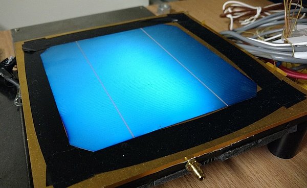
This station consists of an Oriel Sol3A-CPV Class AAA solar simulator with a continuously-adjustable 1-sun intensity over a 30×30 cm2 beam that is collimated with a divergence half-angle of 0.5°. It uses a 1600 W Xe arc lamp with interchangeable filters to achieve different air masses, including the AM1.5G and AM1.5D standard spectra. Both vertical and horizontal illumination is available. This station is most suited to the characterization of bare solar cells, chip-on-carrier receivers, and CPV sub-modules under continuous light simulating the direct-beam component of sunlight.


High-concentration continuous-wave solar simulator and photovoltaic device characterization station:
This station incorporates a Spectrolab XT-30 Class A solar simulator, which was the first of its kind in the world. This artificial sun uses a 3000 W Xe arc lamp at its heart to generate high-concentration light up to >1000 times the intensity of the sun over a uniform beam of up to 1 cm2. An AM1.5D spectral filter ensures a close match to the terrestrial spectrum, further refined via six continuously-variable band filters. Concentrator solar cells and receivers are tested for their current-voltage behavior and related parameters (fill factor, efficiency, etc). The high intensity and continuous illumination of this system allows the investigation of temperature effects and device reliability.


Extreme-concentration flash solar simulator and photovoltaic device characterization station:
This station utilizes an Alpha Omega Power Technologies Gen3 solar simulator, using a Xe arc flash lamp (0.5 Hz) to produce intensities of up to 5000 suns over a uniform beam of 1.5×2.5 cm2. This setup includes tunable filters to achieve current-matching between the subcells of a multi-junction solar cell, and simultaneous monitoring of a reference cell. The current-voltage behavior of bare cells and chip-on-carrier receivers can be characterized over a single 500-μs flash.


High-concentration flash solar simulator and photovoltaic device characterization station:
This station utilizes a Sinton HCCT solar simulator, using a Xe arc flash lamp (0.2 Hz) to produce intensities of up to 2000 suns over an area of ~2.5×2.5 cm2. This setup permits the use of interchangeable filters to achieve the desired current balance across the subcells of a multi-junction solar cell. The current-voltage behavior of bare cells and chip-on-carrier receivers can be characterized with a single IV data-point measured per flash.

Low-concentration continuous-wave solar simulator and photovoltaic device characterization station:
This station incorporates an Oriel 92191 solar simulator, using a 1600 W Xe arc lamp to produce 1-150 times the intensity of the sun over a uniform beam of up to 5×5 cm2. This setup permits the use of several different air mass filters for the simulation of both terrestrial and extraterrestrial spectra, including AM0, AM1, AM1.5G, AM1.5D, and AM2. Both bare cells and chip-on-carrier receivers are characterized on a temperature-controlled platform, permitting the measurement of temperature-dependent performance.


Optoelectronic Characterization
Photoluminescence spectroscopy system:
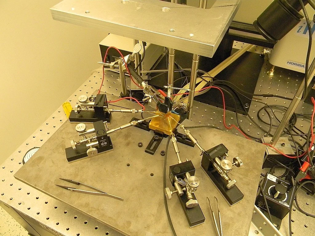
This PL station includes a liquid nitrogen-cooled cryostat for sample excitation under intensity-controlled laser light and temperatures of 77 K and above. Six lasers are available at wavelengths 325, 405, 532, 785, 980, and 1342 nm. A real-time imaging system allows a magnified view of the sample from above, and a view of the whole sample from the side. The sample holder inside the cryostat also allows the use of high magnification objectives which can excite a very small area on the sample while collecting more light for better results (spatially-dependent measurements are made at the micrometer-scale). Collected photoluminescence is directed through a Horiba iHR320 imaging spectrometer to liquid nitrogen-cooled Si and InGaAs detectors which enable low-noise spectral measurements over the wavelength range of 300-1700 nm. Electrical probing allows the measurement of a device's current-voltage characteristics and its electroluminescence.


External and Internal Quantum Efficiency station:
This station studies the response of a solar cell over its entire absorbed wavelength region using a Newport Oriel IQE 200. The external and internal quantum efficiencies, and specular and diffuse reflectances of the cell are measured over wavelengths from 300 to 1800 nm using a Xe arc lamp that is chopped and passes through a monochromator. For measurements of devices with multiple junctions, both voltage and light biasing are provided, the latter using either filtered white light sources or seven independently controlled laser diodes. The cell is electrically probed on a vacuum chuck with temperature control over 0 to 125°C.


Scanning probe microscope with high-resolution electrical modes:
A Bruker Dimension ICON atomic force microscope provides a high-resolution, low-noise platform for contact, tapping, PeakForce tapping, and Dark-Lift tip-to-sample modes. Additionally, this tool provides several powerful electrical scanning modes, including scanning spreading resistance microscopy (SSRM), scanning capacitance microscopy (SCM), scanning voltage microscopy (SVM), and Kelvin probe force microscopy (KPFM).


Photonic power converter testbench:
This flexible testbench is designed around characterizing the optoelectronic performance of photonic power converters (phototransducers) and their integration into various components, such as optically-isolated power supplies (power opto-couplers) and power-over-fiber systems intended for application in smart devices and the Internet of Things. The setup includes several free-space and fiber-coupled lasers, and temperature-controlled chucks for both the light-emitter and photo-converter.A Bruker Dimension ICON atomic force microscope provides a high-resolution, low-noise platform for contact, tapping, PeakForce tapping, and Dark-Lift tip-to-sample modes. Additionally, this tool provides several powerful electrical scanning modes, including scanning spreading resistance microscopy (SSRM), scanning capacitance microscopy (SCM), scanning voltage microscopy (SVM), and Kelvin probe force microscopy (KPFM).


